- ROI (Region of Interest) inspection modes
- Script scanning workflow
- Coordinate-based inspection mode
- Random inspection mode

Non-Destructive TSV Inspection System
● Exclusive optical scanning technology with patented non-destructive defect inspection enables real-time analysis without making physical cross sections.
● AI-assisted precision inspection of TSV side walls ensures accurate defect detection, supporting both blind and through vias.
● TSV quality assessment across the entire functional die on the wafer enables precise quantified evaluation for the die qualification and classification.
● AI-assisted precision inspection of TSV side walls ensures accurate defect detection, supporting both blind and through vias.
● TSV quality assessment across the entire functional die on the wafer enables precise quantified evaluation for the die qualification and classification.
FEATURES
FEATURES
-
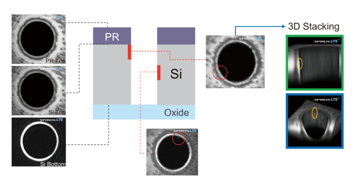
TSV Inner Wall Defect Inspection
Defects such as striations, scallops, and cracks can compromise the insulation layer and lead to leakage currents. -
Defect Data Collection and AI Database Development
Systematic collection and organization of large defect datasets, combined with AI technology to build an intellectual database, enables accurate analysis through quantitative defect inspection standards, optimizing process parameters to enhance product yield and manufacturing efficiency.
Multi-Mode Automatic Inspection with Flexibility
AI-Assisted Detection for TSV Defect Identification
Intuitive User Interface
Automated Loading and Unloading
ADVANTAGES
ADVANTAGES
Non-Destructive Inspection
Non-linear optical inspection and patented SpiroxLTS technology enables precise, quantitative defect evaluation without sample destruction.
Quick Sample Inspection
SP8000S offers a faster and more efficient inspection process compared to traditional cross-sectional scanning electron microscopy (SEM).
Precise Defect Positioning
Precise localization of TSV defects across wafer dies, identifying critical regions and providing essential data for process optimization.

3D Imaging Comparison of TSV Quality
FUNCTION DESCRIPTION
FUNCTION DESCRIPTION
Improving Efficiency and Yield:
Online automated inspection with big data collection reduces SEM sampling, accelerates process optimization, and significantly improves product quality and yield.
Online automated inspection with big data collection reduces SEM sampling, accelerates process optimization, and significantly improves product quality and yield.
Reducing Production Costs:
Reducing defect rates and rework times, thus lowering material waste and production costs.
Reducing defect rates and rework times, thus lowering material waste and production costs.
Enhancing Process Optimization:
Using AI analysis to continuously optimize processes, improving stability and performance.
Using AI analysis to continuously optimize processes, improving stability and performance.
Increasing Market Competitiveness:
Enhancing product reliability and consistency, attracting more customers and collaboration opportunities.
Enhancing product reliability and consistency, attracting more customers and collaboration opportunities.
Data-Driven Decision Making:
Providing precise data analysis to optimize process parameters, enabling quick response to market changes and customer demands.
Providing precise data analysis to optimize process parameters, enabling quick response to market changes and customer demands.
-
Capturing TSV Striation Cross-Section and 3D Imaging
-
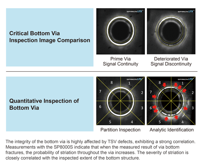
 Bottom TSV Striation Cross-Section and 3D Imaging
PRODUCT SPECIFICATIONS
PRODUCT SPECIFICATIONS
| Item | Content |
|---|---|
| Model Number | SP8000S |
| Model Name | SP8000S Non-destructive TSV Inspection System |
| Key Optical Technology | Nonlinear Optical Inspection (Applicable wavelength range: 1200~1800 nm) |
| Applicable Sample Size | 8” & 12” Wafers |
| Measurement Items | Inspection of various TSV wall defects: striations, scallops, cracks, and evaluation of hole wall quality. |
| Measurement Accuracy |
X/Y Axis Accuracy: < 1.5 µm, Z Axis Accuracy: < 2 µm (@ 20x objective lens, numerical aperture 0.8) |
| FOV / Measurement Time | FOV 400 µm x 400 µm**; 3.5 seconds per frame*** |
| Inspection Mode | Micro-area imaging, automatic region-based measurement, coordinate value automatic measurement, random automatic measurement, and customizable scanning process. |
|
Dimensions and Weight (Tentative) |
L2.3 m x W1.8 m x H1.8 m (Weight: 2600 kg) Automated loading and unloading |
| Electrical Specifications | 220V 60Hz AC 2000W |
** At 20x objective magnification
*** Scanning resolution: 512 x 512 pixels
*** Scanning resolution: 512 x 512 pixels